GLF76311
Nano-Current Consumed Power On/Off Control IC
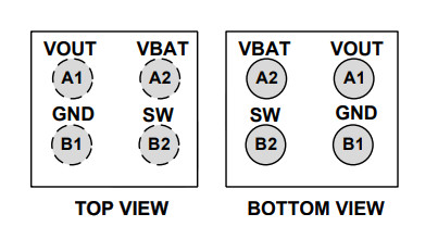
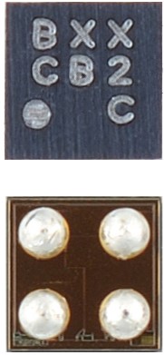
0.97mm x 0.97mm
0.55mm thick
0.5mm pitch
4 bump
WLCSP
Features
- Ultra-Low ISD : 7 nA Typ @ 3.6 VBAT
- Ultra-Low IQ : 6 nA Typ @ 3.6 VBAT
- Low RON : 34 mΩ Typ @ 3.6 VBAT
- IOUT Max : 2 A
- Wide Input Range: 2.5 V to 5.5 V
6 Vabs Max. - Turn-On Delay Time, 3 s Typ.
- Turn-Off Delay Time, 6 s Typ.
- Controlled VOUT Rise Time: 1 ms at 3.6 VBAT
- Integrated Output Discharge Switch When Disabled
- Operating Temperature Range: - 40 to 85 °C
- HBM: 8 kV, CDM: 2 kV
- Ultra-Small: 0.97 mm x 0.97 mm x 0.55 mm WLCSP
Applications
- Smart Devices
- Mobile handheld device
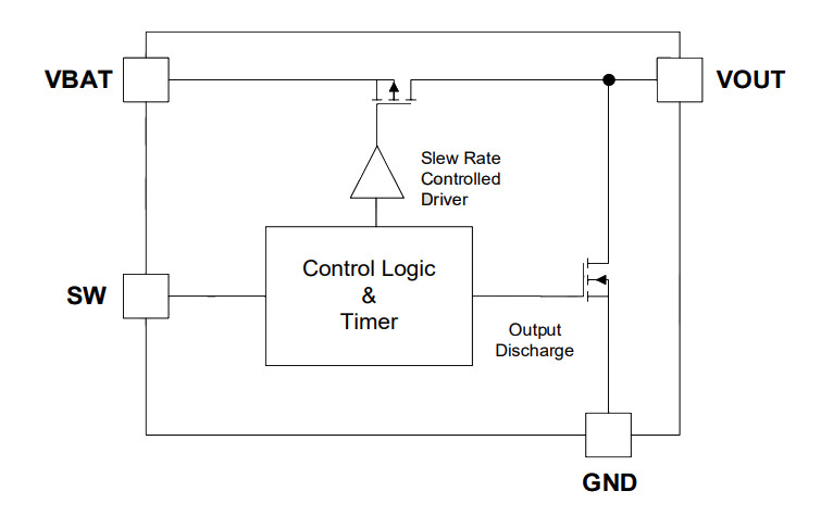
FUNCTIONAL BLOCK SCHEMATIC
APPLICATION SCHEMATIC

PRODUCT DESCRIPTION
The GLF76311 is an ultra-thin, ultra-efficient IQSmartTM load switch with an integrated on and off delay timer for Smart bracelet and Mobile handheld devices.
When the VBAT pin is connected to the battery, the main switch of GLF76311 is turned on, that is the default state. During the normal operation mode, pulling the SW pin to a low level for 6 seconds turns off the GLF76311 and the entire system enters the ultra-deep sleep energy-saving mode.
When the GLF76311 is off, pulling the SW pin to a low level for 3 seconds activates the GLF76311 again and the entire system enters the normal working mode.
The GLF76311 helps to reduce power consumption with the best in class RON, a breakthrough on state IQ of only 6 nA when the switch is on and ultra-low ISD of only 7 nA when switch is off. This switch can help significantly extend the system battery life in mobile devices during shipping or in extended shutdown times.
An integrated 1 ms slew rate control can also enhance system reliability by mitigating bus voltage swings during switching events, where uncontrolled switching can generate high inrush currents that result in voltage droop and/or bus reset events. The GLF slew rate control specifically limits inrush currents during turn-on to minimize voltage droop. The output discharge function makes the output voltage shut off safely.
The GLF76311 is available in 0.97 mm x 0.97 mm x 0.55 mm wafer level chip scale package (WLCSP).

